- Home
- Semiconductors & Electronics
- Kao's cleaner CLEANTHROUGH
- Cleaner for temporary bonding tapes and resists
Cleaner for temporary bonding tapes and resists
Precision cleaner for the fabrication of advanced and
high-density packages
Up until recently and still is, scaling had been the most significant technology for the semiconductor chip production for high performance functional devices. But as the process node is down to less than 10nm and getting closer to the size of the atoms, physical limitation is no doubt to come. In order to enhance the device performance other than by scaling, advanced packaging technology which includes Fan-Out Wafer Level Package(FO-WLP), Fan-Out Panel Level Package(FO-PLP), 2.5D packages with interposers, and finally 3D packages with Through Silicon Via/Through Glass Via(TSV/TGV) and Cu-Cu interconnection, is becoming to be of importance than ever.
To produce those advanced packages, it consists of handling very thin wafers or chips during the process. Temporary bonding/de-bonding(TBDB) technique, where wafers or chips are temporarily bonded onto the carrier such as glass to support the handling in the process is applied for most of the cases. For this temporary bonding materials, resists such as polyimides(PI) and polybenzoxazoles(PBO) or various kind of tapes are being used.
Ultra-clean surface could be obtained by removing even the slight residue
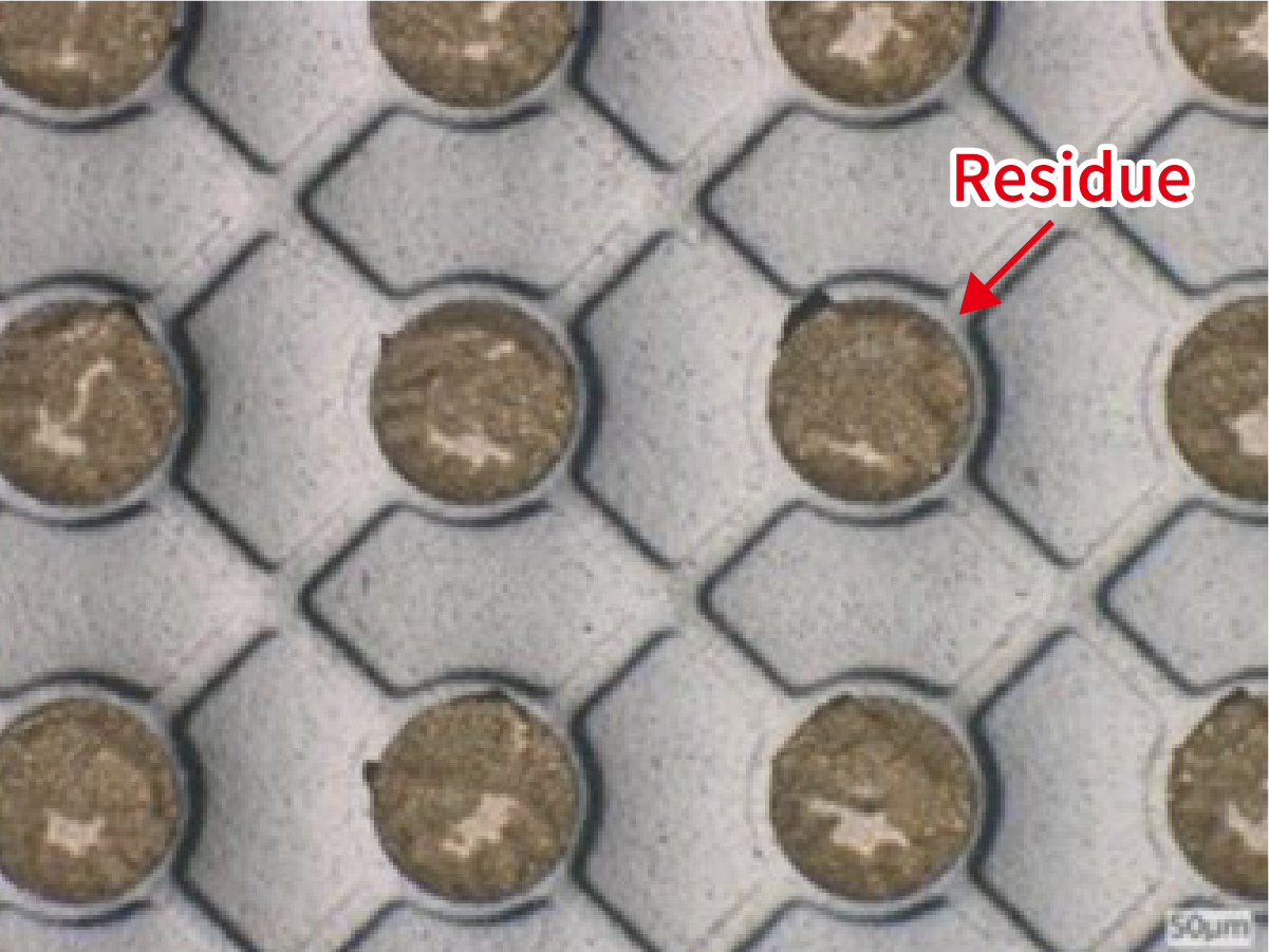
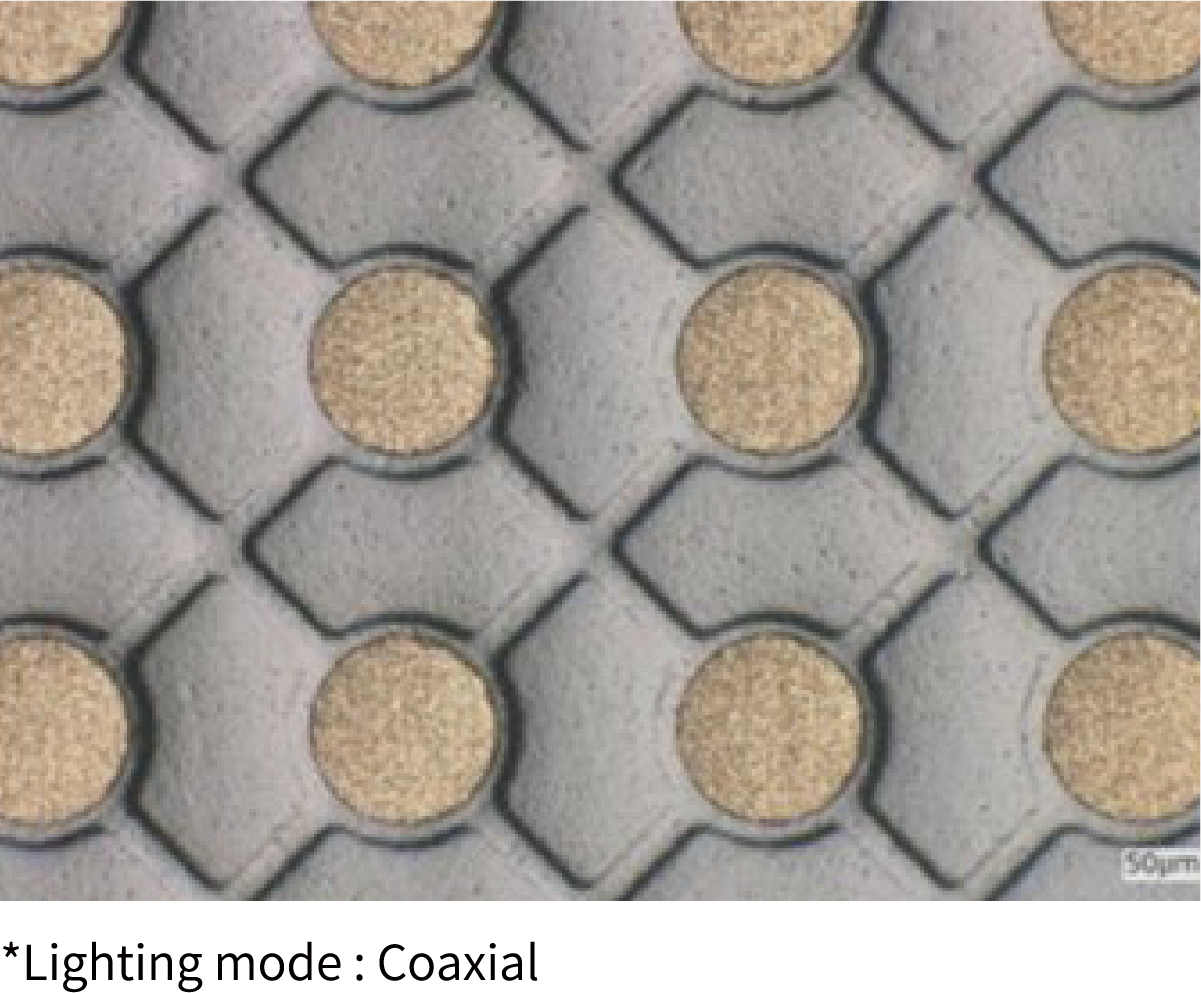
As the slight residue from the temporary bonding materials at TBDB process may lead to the defect during further integration, it is preferred that the material is completely cleaned. However, the materials exposed to strong laser or high temperature are sometimes very difficult to remove.
Kao’s cleaner selectively removes even the slight residue without damaging the peripheral materials, which we hope to enhance the acceleration of advanced packaging technology.


Lineup
| Model | UR series (developing product) | KS-7600K |
|---|---|---|
| Target material | Tapes | Resists |
| Usage | As is used | As is used |
| Feature | Removes tape residues after high temperature or strong laser process. Low damage to the peripheral materials (metals/insulation resins) |
High resist dissolution capability Low damage to the peripheral materials (metals/insulation resins) |
- Home
- Semiconductors & Electronics
- Kao's cleaner CLEANTHROUGH
- Cleaner for temporary bonding tapes and resists


